Logic Gates with VHDL-AMS
by it support 25. März 2015· 5 Min. lesen
In this post it is shown how you can model a logic gate with VHDL-AMS. To explain the basic concept I use a dual 2-input AND gate 74AHC2G08 from NXP [1]. The model is created and simulated with System Vision from Mentor Graphics. You can use this model as a basic for other logic gates.
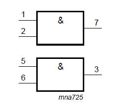
Block Diagram of 74AHC2G08 (from datasheet)
Please find the full source code at the end of the post.
Features
[list type=»check»]
- internal A/D and D/A conversion so you do not need some additional blocks for SPICE compatibility
- Vcc dependend input voltage thresholds
- Vcc dependend output voltages
- propagation delay
- rise and fall time
- schmitt-trigger input which simulates the worst case of the input stage
[/list]
Generic
  generic (
    REL_THRESH_IN_POS	: real := 0.75;		-- relative + input threshold to Vcc
    REL_THRESH_IN_NEG	: real := 0.25;		-- relative - input threshold to Vcc
    REL_OUT_POS		: real := 0.86;		-- realtive + output voltage to Vcc
    REL_OUT_NEG		: real := 0.08;		-- realtive - output voltage to Vcc
    T_RISE		: real := 3.0e-9;	-- rise time of output [s]
    T_FALL		: real := 3.0e-9;	-- fall time of output [s]
    T_DELAY		: real := 12.3ns	-- propagation delay of Gate [s]
  );
The Generic parameters are constant during the simulation. Here is define the relative voltages in depencency to Vcc. In general you should take worst case values. If you want to make a ideal simulation set the output values to 1.0 and 0.0. The ideal trigger should be around 0.5.
Because T_RISE and T_FALL are not defined in the datasheet and are strongly dependend on the load you must set it depending on your environment. In this example they are set to 3ns for the ramp attribute at the output equations.
Port
  port (
    terminal A1, A2, B1, B2, Y1, Y2, VCC, GND: ELECTRICAL
  );
Because the terminals are all electrical, you can use this VHDL-AMS model directly in a SystemVision SPICE netlist without any serperate conversion blocks.
Architecture Declarations
  -- input voltages -- no current will flow
  quantity vVcc across 	VCC to GND;
  quantity vA1 across 	A1 to GND;
  quantity vA2 across 	A2 to GND;
  quantity vB1 across 	B1 to GND;
  quantity vB2 across 	B2 to GND;

  -- output branches
  quantity vY1 across cY1 through	Y1 to GND;
  quantity vY2 across cY2 through	Y2 to GND;

  -- signals
  type voltageArray is Array (natural range <>) of voltage;
  signal vOut, d_vOut	: voltageArray(2 downto 1) := (others => 0.0);
  signal sA, sB		: std_ulogic_vector(2 downto 1) := (others => '0');
All the quantities are refered to the GND pin and not to the electrical_ref so the GND level can be defined outside the model.
Quantities without through declarations do not stress the circuit (no input current).
The declaration of the signals in an array is more efficent especially for devices with more gates.
Input Stage
    -- check logic inputs
    sA(1) <= '1' when vA1'above(vVcc*REL_THRESH_IN_POS)
        else '0' when not vA1'above(vVcc*REL_THRESH_IN_NEG);
    sA(2) <= '1' when vA2'above(vVcc*REL_THRESH_IN_POS)
        else '0' when not vA2'above(vVcc*REL_THRESH_IN_NEG);
    sB(1) <= '1' when vB1'above(vVcc*REL_THRESH_IN_POS)
        else '0' when not vB1'above(vVcc*REL_THRESH_IN_NEG);
    sB(2) <= '1' when vB2'above(vVcc*REL_THRESH_IN_POS)
        else '0' when not vB2'above(vVcc*REL_THRESH_IN_NEG);
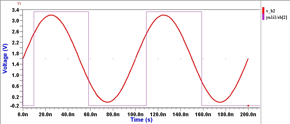
This VDHL-AMS code implements directly a Schmitt-Trigger input. The user should be aware that this does not represent a situation from a real component. But it models the worst cases of both thresholds voltages. In the diagram below you can see the behaviour of the input B2. The violet signal is digital and just represent high and low. It is not adjusted to the voltage at the Y-Axis.
Logic Stage
  -- logic stage
  vOut(1) <= vVcc*REL_OUT_POS when sA(1) = '1' and sB(1) = '1' else vVcc*REL_OUT_NEG;
  vOut(2) <= vVcc*REL_OUT_POS when sA(2) = '1' and sB(2) = '1' else vVcc*REL_OUT_NEG;
The logic stage sets the output signals to either the high or the low output voltage dependend on the digital signals sA and sB. Here can be implemented all different kind of customized logical functions.
Delay Stage
  --delay stage
  d_vOut <= vOut'delayed(T_DELAY);
The signal d_vOut correspondes exactly vOut except it has a delay of T_DELAY. This delay equals the propagation delay of the gate.
Output Stage
  --synchronize the analog core with the digital on change of d_Vout
  break on d_vOut;

  -- output equations
  vY1 == vOut(1)'ramp(T_RISE,T_FALL);
  vY2 == vOut(2)'ramp(T_RISE,T_FALL);
The output quantities are defined by the ramp attribute of the vOut signal. This attribute smooths the digital signal in the time and adjusts signal jumps to ramps.
The break on statement calls the analog simulation core if the digital signal d_vOut changes.
Complete Model Result
So if we set all parts together we get a dual 2-input AND gate. In the following diagram it is shown Input A and B from the channel 1 and the corresponding output Y.

- The first T_DELAY seconds the output stays at 0.0 volts because vVcc initialise with 0.0 volt so the dependend voltages are also 0.0 until the first digital event which invokes a recalculation of the analog core.
- The peak at 80ns is not a failure. It exists because there was a change of the signals T_DELAY before. Because of the ramp and threshold values there was a small overlap.
- This is the propagation delay
If Nr. 1 is distrub your simulation you can get away of it when you implement the delay stage as followed (do not forget the additional declaration).
  -- architecture declatration
  signal sPowerOn      :std_logic := '0';
...
begin
...
  -- delay stage
  sPowerOn <= '1' when vVcc'above(0.1);
  d_vOut <= vOut'delayed(T_DELAY) when sPowerOn = '1' and sPowerOn'stable(T_DELAY)
       else (others => vVcc*REL_OUT_NEG);
Full Source Code
--------------------------------------------------------------------------------
-- Dual 2-Input AND Logic Gate
-- data from NXP 74AHC2G08
--------------------------------------------------------------------------------
library IEEE;
use IEEE.std_logic_1164.all;
use IEEE.ELECTRICAL_SYSTEMS.all;

entity AND_GATE is
  generic (
    REL_THRESH_IN_POS    : real := 0.75;        -- relative + input threshold to Vcc
    REL_THRESH_IN_NEG    : real := 0.25;        -- relative - input threshold to Vcc
    REL_OUT_POS          : real := 0.86;        -- realtive + output voltage to Vcc
    REL_OUT_NEG          : real := 0.08;        -- realtive - output voltage to Vcc
    T_RISE               : real := 3.0e-9;    -- rise time of output [s]
    T_FALL               : real := 3.0e-9;    -- fall time of output [s]
    T_DELAY              : time := 12.3ns    -- propagation delay of Gate [s]
  );
  port (
    terminal A1: ELECTRICAL;
    terminal A2: ELECTRICAL;
    terminal B1: ELECTRICAL;
    terminal B2: ELECTRICAL;
    terminal Y1: ELECTRICAL;
    terminal Y2: ELECTRICAL;
    terminal VCC: ELECTRICAL;
    terminal GND: ELECTRICAL
  );

end entity AND_GATE;

architecture default of AND_GATE is
-- input voltages -- no current will flow
    quantity vVcc across     VCC to GND;
    quantity vA1 across     A1 to GND;
    quantity vA2 across     A2 to GND;
    quantity vB1 across     B1 to GND;
    quantity vB2 across     B2 to GND;

    -- output branches
    quantity vY1 across cY1 through    Y1 to GND;
    quantity vY2 across cY2 through    Y2 to GND;

    -- digital signals and voltages
    type voltageArray is Array (natural range <>) of voltage;
      signal vOut, d_vOut  : voltageArray(2 downto 1) := (others => 0.0);
      signal sA, sB        : std_ulogic_vector(2 downto 1) := (others => 'U');

begin
    -- check logic inputs
    sA(1) <= '1' when vA1'above(vVcc*REL_THRESH_IN_POS)
        else '0' when not vA1'above(vVcc*REL_THRESH_IN_NEG);
    sA(2) <= '1' when vA2'above(vVcc*REL_THRESH_IN_POS)
        else '0' when not vA2'above(vVcc*REL_THRESH_IN_NEG);
    sB(1) <= '1' when vB1'above(vVcc*REL_THRESH_IN_POS)
        else '0' when not vB1'above(vVcc*REL_THRESH_IN_NEG);
    sB(2) <= '1' when vB2'above(vVcc*REL_THRESH_IN_POS)
        else '0' when not vB2'above(vVcc*REL_THRESH_IN_NEG);

    -- logic stage
    vOut(1) <= vVcc*REL_OUT_POS when sA(1) = '1' and sB(1) = '1' else vVcc*REL_OUT_NEG;
    vOut(2) <= vVcc*REL_OUT_POS when sA(2) = '1' and sB(2) = '1' else vVcc*REL_OUT_NEG;

    --delay stage
    d_vOut <= vOut'delayed(T_DELAY);

    --synchronize the analog core with the digital on change of d_Vout
    break on d_vOut;

    -- output equations
    vY1 == d_vOut(1)'ramp(T_RISE,T_FALL);
    vY2 == d_vOut(2)'ramp(T_RISE,T_FALL);

end architecture default;
Conclusion
This post should serve as basics for logic ICs modulation with VHDL-AMS. Only with some simple adjustements you have the oportunity to create a lot of different ICs. For example duplicate the channels for AND gates with more channels or change the logic function for other gate types.
Beside that it gives some application ideas for VHDL-AMS models and the handling of quantities.
Schreiben Sie einen Kommentar